CHALLENGES IN DYNAMIC FLEXIBLE CIRCUIT BOARD DESIGN
Dynamic flexible circuit boards have the capability of solving many interconnect and packaging challenges in designs that require repetitive motion. They allow for extremely high-density interconnects while consuming a very small amount of space. However, these applications have a different WHERE set of design rules than that of a “one-time” or “bend-to-fit” static application.
Due to the repetitive bending requirements, the design must be configured so that the copper circuits do not exceed the extent of their ductility. If this occurs the copper will start to harden, loose its ductility, eventually creating cracks in the circuits and the resulting open circuits.
Minimum Bend Radius
The minimum bend radius is critical to the success of a dynamic flex circuit application. The rule of thumb is a minimum of 100X the finished thickness of the circuit in the dynamic flex area. Some flexible PCB designs may have both static and dynamic flex areas, and as such, the design rules will differ between the two types of areas. As an example, a flex circuit with a finished thickness of 0.005” will need a 0.500” minimum bend radius or 1.000” minimum bend diameter to ensure its long-term reliability over an infinite number of cycles. The minimum bend radius can be adjusted by the choice of material thicknesses used in the design. Thinner copper combined with a thinner core and coverlay layers will reduce the minimum bend radius capability, but at potentially added costs.

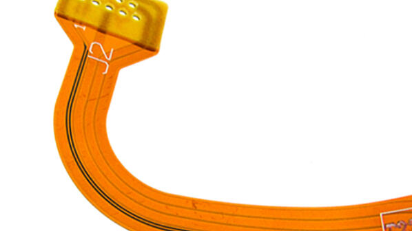
Flexible PCB manufactured with the proper bend radius.
Common applications for dynamic flex circuit designs are print head interconnects, rotating scanning assemblies, flip up display interconnects, rotating/linear actuators, etc.
Copper Type And Grain Orientation
For flexible circuit board designs, there are two types of copper available:
1.Electro-deposited (ED)
2.Rolled annealed (RA).
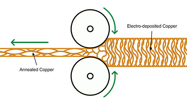
RA copper starts as ED copper, and when subjected to the rolled annealed process has its grain structure transformed from the initial vertical grain structure of ED copper to an elongated and horizontal structure. This increases the ductility of the copper, allowing it to better withstand the effects of work hardening and avoid the formation of micro cracks in the vertical axis. This process also results in the copper having a grain direction due to the elongation of the grain structure.

Example of copper being subjected to the rolled annealed process.
Dynamic flex applications must utilize RA copper with the grain direction oriented in the length of the flex circuit. This provides the highest degree of ductility in the direction of the bend requirement.
RA copper is available in a variety of thicknesses ranging from ? ounces up to 2 ounces with ? ounce and 1 ounce being the most commonly used.
Layer Count, Neutral Bend Axis And Gerber Layout Requirements
Layer counts are limited in a dynamic flex circuit application as per IPC 2223 design guide recommendations.
The optimum configuration is a 1-layer construction. This allows the copper circuits to be in the center of the construction, also referred to as the neutral bend axis, which results in the copper being subjected to the least amount of compressive and tensile forces possible.
A 2-layer construction is allowable providing that a thin adhesive less flex core, 0.001” or less, is used between the two layers. This minimizes the distance that the circuits are located away from the neutral bend axis thus minimizing stresses imparted during bending. It is also recommended to avoid solid or cross hatched fills and to stagger the traces in relation to each other from layer to layer to minimize the I-beam effect.
Three-layer and greater designs, in general, are not recommended for dynamic applications or if used must have minimum bend radiuses much greater than 100X.
Shielding Requirements For EMI And RF Purposes
For dynamic flexible PCB applications that require shielding for EMI or RF purposes, the preferred solution is to use shielding films rather than adding a copper or silver ink layer. Both add significant thickness to the design and limit the bend capabilities. Shielding films are very effective shields, very thin (approx. 17-22 um), highly flexible, and can be attached to one or both sides of a 1- or 2-layer flex circuit.
Shielding films use an electrically conductive adhesive to interconnect to a ground circuit through selective openings in the coverlay. For a 2-layer design, non-plated holes allow the two shield layers to interconnect to one another.
Summary
Dynamic flex circuit applications solve a very wide variety of packaging challenges and create design opportunities that no other interconnect method can provide. Following the recommended design rules and material selection will ensure a successful and reliable design.
Capabilities
Payment Methods
Specials Price
Carriers
Support Hobbyist
Certificate
Customer Support
Follow Us
Tel: 1-905-339-2881
Email: [email protected] , [email protected]
Copyright Gold Phoenix PCB Co., Ltd. 2011 - 2025
Tel: 1-905-339-2881 Email: [email protected] , [email protected]
Quality Control System
|
Products/Service
|
Friendly Links
Copyright Gold Phoenix PCB Co., Ltd. 2011 - 2025


