Blind & Buried Vias
Due to the increasing complexity of design structures blind vias and buried vias are increasingly used in high-density circuit boards. Blind and buried vias are used to connect between layers of a PCB WHERE space is at a premium.
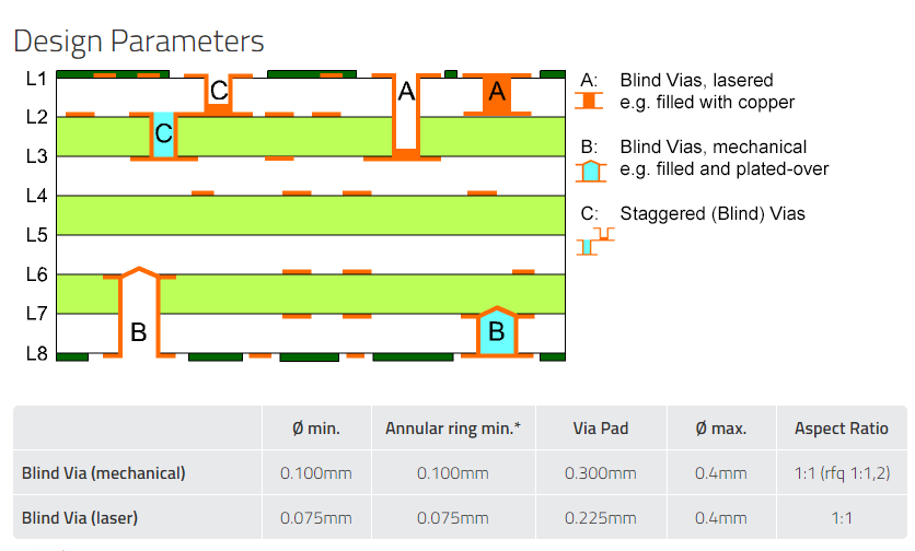
Blind Via
Blind vias are used to connect one outer layer with at least one inner layer. The holes for each connection level must be defined as a separate drill file. The ratio of hole depth to drill diameter (aspect ratio) must be ≤ 1. The smallest hole determines the depth and thus the max. distance between the outer layer and the corresponding inner layers.
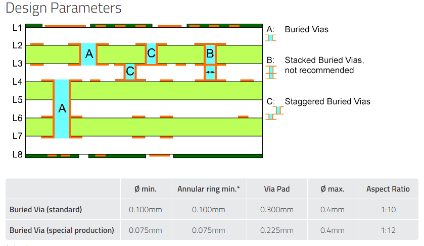
Buried Via
Buried vias are used to create connections of the inner layers, which have no contact with the outer layers. The holes for each connection level must be defined as a separate drill file. The ratio of hole depth to drill diameter (aspect ratio) must be ≤ 12. The smallest hole determines the depth and thus the max. distance between the respective inner layers.
How to Use Blind and Buried Vias in Altium Designer
Working through fabrication, assembly, and manufacturing, you’ll want to make sure your layout is accurate and secure. Material and plating chosen, solder planned, components and prototype estimations acquired, and any other board requirements you may have. Blind and buried vias in Altium Designer are regular vias that are set up to span specific layers instead of the full layer stack. Therefore to understand how to set up and use blind and buried vias, you must first know how to work with a regular via.
In Altium Designer padstacks and vias are design objects created by defining their attributes. You specify their size, hole size, tolerances, and other attributes in order to complete their creation. They can be created from templates or you can define them yourself on the fly. Below is a picture of the default via set up in the PCB preferences menu.
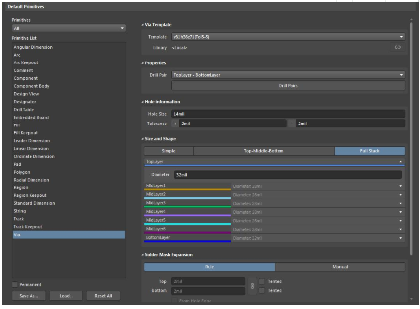
You can see above the template that was used for the default via, the hole information, and the via size information. You can also see how Altium Designer gives you control over the details of the via by setting it up according to the following criteria:
1.Simple: One size for all layers.
2.Top-Middle-Bottom: You can specify individual sizes for the top, middle, or bottom.
3.Full Stack: You can set up sizes on all layers individually.
When you place a via without it being attached to a net, Altium Designer will use the default via in your design as shown above. You also have the ability to set specific vias to be used with specific nets, net classes, and other criteria. To do this you will set up via routing rules from the “Design > Rules” pull-down menu as shown below.
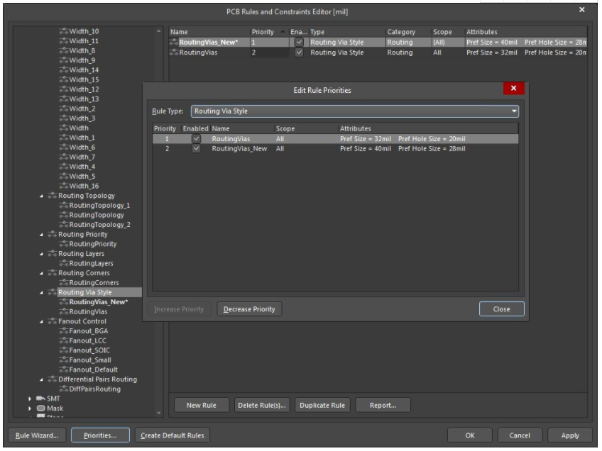
In the picture above, you can see the “Routing Via Style” rules category with two different rules in it. You can see that these rules already have via attributes assigned and these rules can also have their priority changed as shown above. You can create as many rules as you need and prioritize them as necessary
To set the size of the via in the rule, you can accomplish this by below way. As shown in the top of the picture below, you can see that within the constraints section we have selected “Min/Max Preferred”. In this way you can define the size of the via on the fly while setting up your rule.
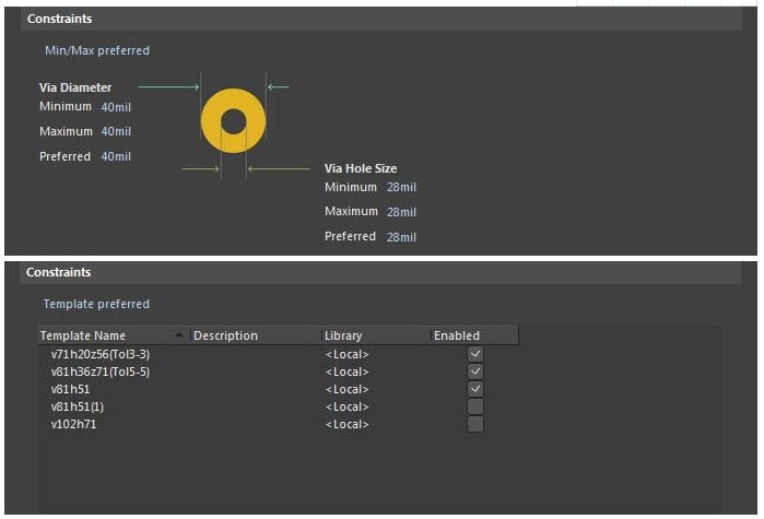
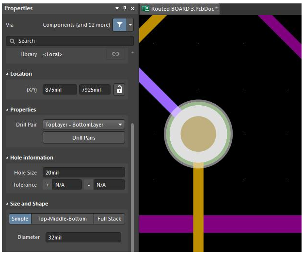
As you route, the routing rules that you defined for the net class will determine the via that gets used. You also though have the ability to change the via on the fly while routing. Once a via has been instantiated on the board you can access its properties by right clicking on the via and selecting “Properties”. In the via properties panel you can change the size, shape, hole size, and other parameters as shown in the picture below.
Configuring Altium Designer for Blind and Buried Vias
Now that we’re all up to speed on working with regular thru-hole vias in Altium Designer, let’s take a closer look at what it takes to work with a blind or buried via. A blind or buried via is going to be similar to a regular via except it will be constrained to a specific span of layers. Since a blind via starts on a surface layer and then penetrates only partially through the board layer stack as shown by first pointer in the picture below, it needs to be started and stopped on those specific layers.
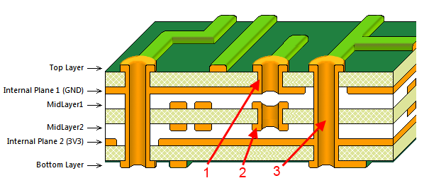
Similarly a buried via also starts and stops on specific layers, but it doesn’t extend to either of the surface layers as shown by the second pointer in the picture above. For comparison you can see how both of these appear next to a regular thru-hole via in shown by the third pointer.
In order to control these layers for the blind and buried vias to start and stop on, you will use the drill pair manager in Altium Designer. The drill pairs that you add is what tells Altium Designer that blind and buried vias are in use, and what the specific start and stop layers are. The “Drill-Pair Manager” in the picture below can be accessed through the “Layer Stack Manager” in the “Design” pulldown menu, or you can also access it directly through the properties panel for a selected via.
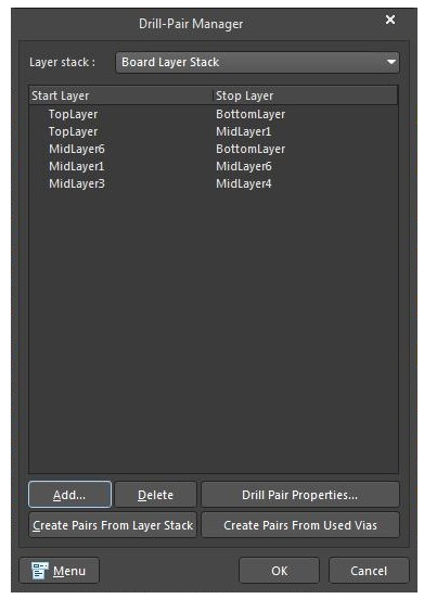
As you can see above, the drill pair manager is configured for a number of different blind and buried vias. There is a blind via configured for top layer down to the first internal layer (MidLayer1), and another blind via configured on the bottom side as well. There are also two buried vias, one configured for MidLayer1 to MidLayer6 and the other for MidLayer3 to MidLayer4. Once you’ve set these drill pairs up, close the “Drill-Pair Manager” dialog box and Altium Designer will be updated with the new drill pair configurations.
Using Blind and Buried Vias in Altium Designer
Now you are ready to start using blind and buried vias, and here is where all of that work you did setting up net classes will really come in handy. Often you will have specific nets that you want to classify for blind and buried vias due to their routing density and purpose. You can easily set up your net classes for routing on specific layers that are intended for a blind or buried via, and set up via rule priorities as well.
When routing you will instantiate your vias in the regular way, by using the “*” key to start a via and then with repeated clicks descend through each layer. You can also use the Ctrl_Shift_Roll mouse wheel combination to descend up or down through each layer as well.
The layer that you start your via on will determine what blind or buried via that will be used. If the layers spanned by the blind or buried via isn’t what you want, use the property panel to change the via drill pair to a different pair. Altium Designer will display blind and buried vias with a split color on them so that you can easily tell which layer the via starts and stops on.
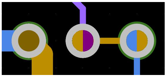
In the picture above you have a thru-hole via on the left with a solid colored core. The via in the middle is a buried via and it starts on a yellow colored layer (MidLayer1) and stops on a purple layer (MidLayer6). The via on the right is a blind via and it starts on a blue colored layer (TopLayer) and stops on the yellow colored layer (MidLayer1).
Once you’ve placed your blind or buried via you can edit it or move it by dragging it around as you can with any other via. Simply grab it with the mouse and move it as shown in the picture below.
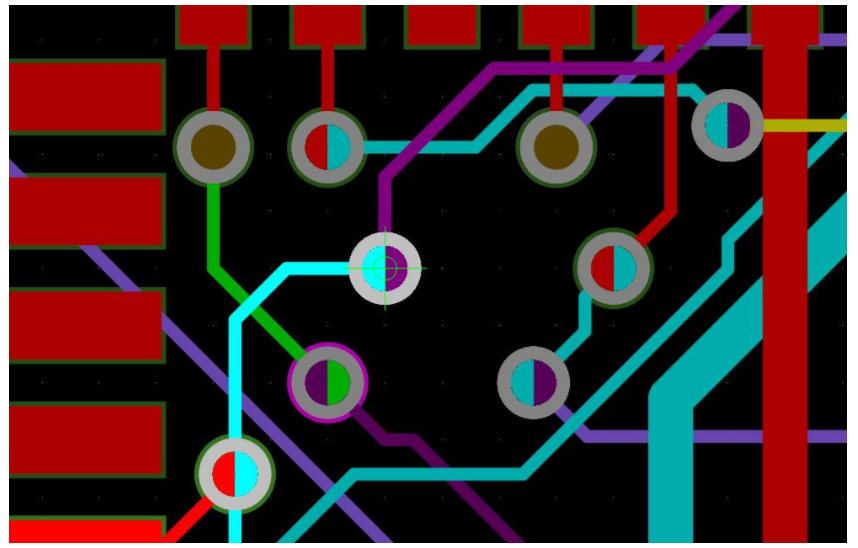
Blind and buried vias can be an extremely useful tool to use when routing your PCB designs. They will open up new options for your routing and allow you to achieve a greater routing density. With the power and functionality in Altium Designer, you will be able to easily work with blind and buried vias.
Capabilities
Payment Methods
Specials Price
Carriers
Support Hobbyist
Certificate
Customer Support
Follow Us
Tel: 1-905-339-2881
Email: [email protected] , [email protected]
Copyright Gold Phoenix PCB Co., Ltd. 2011 - 2025
Tel: 1-905-339-2881 Email: [email protected] , [email protected]
Quality Control System
|
Products/Service
|
Friendly Links
Copyright Gold Phoenix PCB Co., Ltd. 2011 - 2025


