VIA HOLES IN FLEXIBLE DESIGNS
Devices are becoming smaller and thinner, requiring circuit boards that can fit into the equipment without adding any additional weight while being flexible enough to route around components. Flexible printed circuit boards offer high-density electrical connections while also reducing space.
Along the circuit board, flexible films and conductive materials are placed in layers. The number of layers used is dependent on the complexity of the design. To connect the electrical signal between the varying layers, a via hole is placed on the PCB.
Vias Holes In Flexible PCB Areas
Via holes, simply called vias, are holes that are used to make electrical connections between the layers of the design. Vias also come in a variety of shapes and types, such as through-hole, buried vias, blind vias, and microvias.
To create a via, a copper pad is placed at a specific location on each layer of the printed circuit board. The via hole is then drilled through the copper pad on each layer. Chemicals are used to dissolve any remaining epoxy and burrs in the holes as well as to expose the copper pads in the internal layers of the flex circuit. The flexible PCB then undergoes a plating process where a copper coating is chemically added into the holes in a process called electroless copper deposition before the entire board experiences a copper electroplating process and chemical bath cleanings. Lastly, etch resist is added onto the layers to define the circuit patterns the balance of the copper is chemically removed (etched).
Pros:
When it comes to using vias in flexible circuit boards, the main advantage is that they allow for higher complexity circuit routing. The vias route the circuitry through multiple layers throughout the design.
Cons:
If dealing with a device that requires complex circuit boards with multiple layers, manufacturers who must drill in vias may increase their production costs due to this potential complexity. Having a lot of vias also increase the potential of damaging the board during assembly, which may result in the need to scrap the flex circuit and create a new design. Depending on the placement of the vias, they can interfere with other nearby components and take up space that other components require depending on the number of vias that are used.

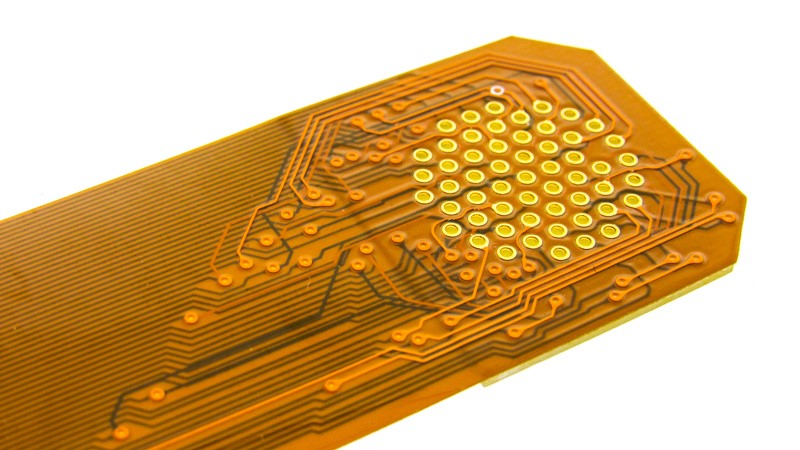
Example of a 2-layer flex circuit with vias.
Overview Of Flexible PCB Areas
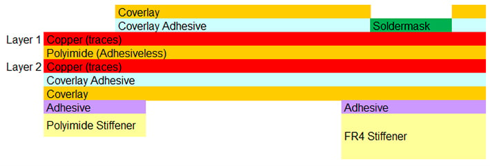
The flexible areas of the flex circuit are made up of polyimide substrates, adhesives, traces, and coverlays.
Polyimide Substrate Film: Polyimide materials make up the dielectric substrate/core layer of the flexible part of the circuit board. This material forms the base where all the traces, vias, and other components are attached. Polyimide is the preferred material due to its flexibility, resilience, temperature resistance, and dielectric properties.
Traces: The traces are the copper electrical conductors on the PCB that allow the signals to move along the circuits. For multi-layer flexible circuit boards, the traces are on multiple layers and staggered in relation to each layer if possible. The widest possible trace is desired and should be covered to allow the flex circuit to bend. This feature ensures the longevity and performance of the circuit board. In addition, rolled annealed copper is preferred over electro-deposited copper for its improved ductility.
Adhesive Materials: Adhesive materials are used to join all the individual layers of the PCB together. The types of adhesive materials used are either flexible epoxy resin or acrylic based.
Coverlay/Cover Coat: Coverlay is used as the external protective covering on the flex circuit. This coverlay, polyimide, is used in place of solder mask as it offers greater flexibility to this area while offering protection to the copper structures.
Solder Mask: Solder mask is a photo-imaged liquid epoxy that can be applied to the bottom and top of the FPCB. It protects the copper from exposure and oxidation. The difference between solder mask and coverlay is that solder mask is liquid-based, and the coverlay is a solid polyimide layer with an adhesive.

Example of flex PCB circuit material stack-up.
Capabilities
Payment Methods
Specials Price
Carriers
Support Hobbyist
Certificate
Customer Support
Follow Us
Tel: 1-905-339-2881
Email: [email protected] , [email protected]
Copyright Gold Phoenix PCB Co., Ltd. 2011 - 2025
Tel: 1-905-339-2881 Email: [email protected] , [email protected]
Quality Control System
|
Products/Service
|
Friendly Links
Copyright Gold Phoenix PCB Co., Ltd. 2011 - 2025


